Materials science literature
Downloads: materials science (carbon, 2D materials and nanotechnology)
-
 Application summary: Raman measurements on graphene
The high specifity of inVia enables graphene to be easily differentiated from other materials, including carbon allotropes such as carbon nanotube and diamond.
-
 Application note: Analyse 2D materials with the inVia Qontor confocal Raman microscope
With so many unique properties, working with 2D materials can be challenging. Whether it is large regions, uneven samples, or small discrete flakes, Renishaw’s inVia Qontor confocal Raman microscope gives you reliable results, quickly and easily.
-
 Product note: Rayleigh imaging using the inVia™ confocal Raman microscope
Product note detailing how you can perform Rayleigh imaging on the inVia confocal Raman microscope.
Downloads: materials science (semiconductors)
-
 Application note: Photocurrent measurements on the inVia™ confocal Raman microscope
When light interacts with semiconducting materials it can induce electrical currents (‘photocurrents’). These currents carry information about the electronic, optical, and charge transport properties of the material. This information is complementary to that obtainable from Raman scattering, which can identify physical changes in the material properties. This application note demonstrates the capability to simultaneously collect Raman and photocurrent data using the photocurrent mapping module concurrently with an inVia Raman microscope.
-
 Application note: Analyse compound semiconductors with the inVia™ Raman microscope
Over the last decade compound semiconductors have attracted a great deal of attention because they offer properties suitable for next generation devices in a wide range of application areas. Historically, the fabrication of these devices has been hindered by material challenges. While these have mainly been conquered at the research level, problems still persist when scaling up to industrial production. Renishaw’s inVia Raman microscope is a non-invasive, non-destructive characterisation tool which provides sub-micrometre information on the vibrational, crystal and electronic structure of materials.
-
 Application note: Analyse silicon carbide (SiC) with the inVia Raman microscope
The properties of silicon carbide are highly dependent on its crystal structure (it can exist in many polytypes), on the quality of the crystal, and on the number and types of defects present. Manufacturers of silicon carbide raw material and devices need to monitor and control these attributes to enhance yield. The first step in controlling these parameters is to measure them repeatably and quantifiably. Renishaw’s Raman systems are ideal for this.
-
 News release: Identifying imperfections with Raman spectroscopy
An article in Compound Semiconductor magazine, October 2015, describes how Raman spectroscopy allows routine mapping of SiC wafers in little more than an hour.
Downloads: materials science (photovoltaics)
-
 Application note: Photocurrent measurements on the inVia™ confocal Raman microscope
When light interacts with semiconducting materials it can induce electrical currents (‘photocurrents’). These currents carry information about the electronic, optical, and charge transport properties of the material. This information is complementary to that obtainable from Raman scattering, which can identify physical changes in the material properties. This application note demonstrates the capability to simultaneously collect Raman and photocurrent data using the photocurrent mapping module concurrently with an inVia Raman microscope.
[1.6MB] -
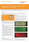 Poster: Simultaneous photocurrent and Raman mapping of single crystalline silicon solar cell modules
A poster demonstrating the inVia's capabilities at studying the efficiency of solar cells against the quality of their manufacture.
[914kB]
Download an application note
-
 Flyer: In-situ and operando Raman spectroscopy for batteries
Renishaw’s inVia™ confocal Raman microscope and Virsa™ Raman analyser are trusted by leading researchers working on battery technology.
-
 Application note: Analyse lithium-ion batteries with the inVia™ confocal Raman microscope
Chemically characterise lithium-ion batteries with Renishaw’s inVia Raman microscope. inVia is the ultimate system for studies ranging from fundamental research on the materials involved through to final product quality control and failure analysis.
-
 Application note: Analyse Li-ion battery anodes with the inVia™ confocal Raman microscope
The inVia confocal Raman microscope is ideal for locating, discriminating, and quantifying the different forms of carbon present in anodes, even those with subtle variations in structure.
Application examples
We have also produced a range of application examples, including the following.
If you would like to find out more, please contact your local representative using the button below, quoting the relevant document reference.
| Document reference | Document description |
| AS001 | SEM-SCA identification of residue on a steel component Steel components that had exhibited poor in-service wear resistance were provided to identify the nature of a suspicious residue noted during stereo optical microscopy observation. In-SEM Raman spectroscopy determined that the residue comprised a paste containing particulates – the particles were identified as diamond (characterised by a band at 1333 cm-1), and the carrier paste as an organic substance. The residue is most likely the remains of polishing compound. |
| AS007 | Common substrate spectra using different laser excitation wavelengths This document provides information on the suitability of various common substrates when preparing a sample for Raman analysis. Some common substrates can provide complex backgrounds, which can complicate the interpretation of Raman bands from the sample. It is therefore important to understand which option is the most appropriate for a given sample and excitation configuration. |
| AS026 | Probe interlayer interactions in graphene Open new research opportunities by investigating interlayer interactions in graphene and other two dimensional crystals, using an inVia Raman microscope equipped with Eclipse filters. |
| AS027 | See sub-diffraction limit graphene features using tip enhanced Raman spectroscopy Reveal highly detailed graphene information by performing tip enhanced Raman spectroscopy (TERS) using inVia combined with an AFM. TERS uses a special plasmonic tip to increase the local electric field at the sample which, in turn, increases the Raman intensity. |
| AS028 | TERS of a malachite green monolayer Analyse minute sample volumes and weak Raman scatterers using inVia and TERS. Tip enhanced Raman spectroscopy (TERS) uses a special plasmonic tip to increase the electric field at the sample which, in turn, increases the Raman intensity. These tips are very small, with diameters on the order of 10 nm to 100 nm, and are held in contact with the sample using a scanning probe microscope (SPM) or atomic force microscope (AFM). |
| AS030 | Raman imaging analysis of graphene flakes Identify the number of graphene layers present in your sample quickly and easily using StreamLine imaging. |
| AS033 | Locate and characterise defects in SiC Learn more about the defects in SiC using StreamLineHR 3D imaging. Raman spectroscopy is a powerful tool for investigating SiC. |
| AS035 | Visualise polytype, strain/stress and nitrogen concentrations in SiC using inVia Use StreamLineHR to image polytype, strain/stress and nitrogen doping in SiC. |
| AS039 | Raman measurements on graphene The high specifity of inVia enables graphene to be easily differentiated from other materials, including carbon allotropes such as carbon nanotube and diamond. |
| AS060 | Characterising DLC with combined in situ Raman spectroscopy and nanoindentation Renishaw and Hysitron have combined an inVia confocal Raman microscope with TI 950 Tribolndenter, producing a system with the capability to directly correlate mechanical properties measurements with comprehensive chemical analyse, in situ. |


