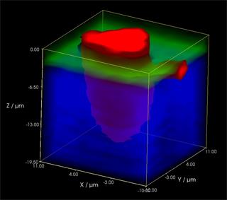
Silicon carbide
Modern electronics use a wide range of semiconductor materials. Cutting edge devices, such as transistors, solar cells and light emitting diodes, push materials properties to their limits, and require extremely homogeneous source materials. Raman spectroscopy is an ideal tool for studying semiconductors.
Characterise semiconductors
You can use Raman to characterise and generate images of all semiconductors (e.g. Si, carbon-based, III-V's, and polymers) and superconductors. A wide range of information can be revealed, including:
- chemical composition (e.g. alloy fractions of compound semiconductors)
- polytypes (e.g. 4H-SiC and 6H-SicC)
- strain/stress
- dopant concentrations
- thin film thickness
- crystal structure type and orientation
- crystal quality
- uniformity and purity
- device temperature
Easy analysis
Raman analysis is simple because it requires no sample preparation. It does not require vacuum technology, or suffer from charging effects experienced with electron microscopy.
Renishaw can configure your Raman system to suit all users, from research scientists to technicians.
Large area analysis
Renishaw Raman systems can analyse very large samples. For example, you can generate images of entire wafers to discover contaminants or residual stresses.
PL characterisation
Renishaw's Raman systems also enable you to collect and analyse photoluminescence (PL) spectra. You can collect both vibrational and electronic information with one instrument.
Online systems
Add Renishaw's Raman systems to your production line to conduct online analysis for quality control purposes. Diagnose problems early, reduce waste and improve yield.
Reliable results
Renishaw's Raman systems produce highly repeatable data that accurately represents the sample. In-built automated calibration and health checking ensure data can be accurately compared, no matter when collected.
Further information
-
 Application note: Analyse silicon carbide (SiC) with the inVia Raman microscope
The properties of silicon carbide are highly dependent on its crystal structure (it can exist in many polytypes), on the quality of the crystal, and on the number and types of defects present. Manufacturers of silicon carbide raw material and devices need to monitor and control these attributes to enhance yield. The first step in controlling these parameters is to measure them repeatably and quantifiably. Renishaw’s Raman systems are ideal for this.
Read an article from Compound Semiconductor magazine
-
 News release: Identifying imperfections with Raman spectroscopy
An article in Compound Semiconductor magazine, October 2015, describes how Raman spectroscopy allows routine mapping of SiC wafers in little more than an hour.
Find out more
Contact your local Renishaw representative today to find out how Renishaw's inVia can provide you with repeatable, reliable results.


