Overcoming the limitations of Raman spectroscopy
You can get the best Raman data possible with some simple solutions. Consider using SERS or TERS to enhance the sensitivity and spatial resolution of Raman scattering.
Raman spectroscopy is a versatile analytical technique for chemical and structural characterisation. We discuss some challenges and disadvantages encountered during Raman analysis, and the solutions to these problems. We also discuss the factors that influence spatial resolution. To achieve a spatial resolution down to nanometres, we can use tip-enhanced Raman spectroscopy (TERS).
Challenges and considerations in applying Raman spectroscopy
Despite the many advantages of Raman spectroscopy, we sometimes need to overcome some practical challenges. These issues are applicable to all Raman instruments. We have solutions so that you can get the best results from your Raman system.
Here are some practical solutions and advice.
1. The Raman effect is relatively weak
Renishaw's Raman systems use highly efficient optical designs and ultra-sensitive detectors.
2. Strong fluorescence backgrounds can mask Raman bands
By using a multiple laser system you can switch to a different excitation wavelength. For example, switching from a visible to a near-infrared laser (e.g. 785 nm) usually reduces fluorescence. This improves your chances of producing spectra with clear Raman bands.
3. Many sample surfaces are not flat
In the past, Raman imaging on uneven samples was difficult. Now, with LiveTrack focus-tracking technology, Renishaws Raman microscopes can automatically stay in focus while collecting data. You can easily study how chemistry and structure changes with topography.
4. Glass containers and microscope slides can mask the Raman bands of your samples
a. Replace glass microscope slides with stainless steel slides.
b. For biological cells, you can use mirror-polished stainless steel, CaF2 or MgF2 microscope slides.
c. Replace standard glass containers with quartz, which produces a lower background at 785 nm than standard glass.
5. Containers and substrates can contribute to your spectrum
You can control the degree of confocality on the inVia™ confocal Raman microscope and the Virsa™ Raman analyser. Combine a high numerical aperture (N.A.) microscope objective with a highly confocal instrument setting to minimise the sampling volume. This helps to counteract any unwanted background contributions from substrate or container materials.
To analyse a bulk sample in a transparent container, you could use a low-NA lens to focus into the vessel. This is another way of maximising the Raman signal from the material of interest and minimising spectral contributions from the container.
6. High laser powers can damage samples
We use lasers to generate Raman scattering. The Raman signal is proportional to the amount of laser power, so more power usually produces a stronger signal.
However, all samples have a laser power density threshold beyond which structural or chemical changes may happen. Here are our solutions:
a. High-throughput spectrometer design; you can produce the highest Raman signals with very low laser powers.
b. Laser power is software controlled and repeatable. In this way, you can be sure that your sample has not changed.
c. Spread the incident laser power over a larger area using line focus mode. You can do this with an inVia microscope, an RA802 Pharmaceutical analyser and an RA816 Biological analyser.
7. Automatically remove cosmic ray features with WiRE™ software
Cosmic rays are high-energy particles from beyond the Earth's atmosphere. If cosmic rays impact a detector during data collection, high-intensity spikes appear in the spectra. Large Raman images can often contain thousands of cosmic ray artefacts.
WiRE software can fully automate the removal of cosmic rays from large Raman images, containing up to 50 million spectra. We can then automate our data analysis workflow to produce reliable results.
The spatial resolution of a Raman image
A few factors determine the spatial resolution of a Raman microscope:
• Laser spot size
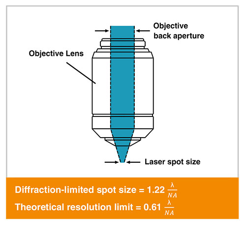
This is a function of the objective's numerical aperture (N.A.) and the laser wavelength. Briefly, higher N.A. and shorter wavelengths produce smaller spot sizes.
• Spacing between spectral acquisition points on the sample (sampling)
This is a function of the sample stage. Renishaw's MS30 high speed encoded stage has a large travel range with small step sizes down to 50 nm. These step sizes are smaller than the smallest diffraction-limited laser spot size.
• The magnification of the optics in the spectrometer and the size of the CCD pixels.
Ultimately this is limited by the inherent wavelike nature of light, to a little under a micrometre.

Equations for calculating the Abbe diffraction-limited spot size and the theoretical lateral resolution limit for a given microscope objective and wavelength of light.
eBook download: Raman spectroscopy explained
- What is the Raman effect?
- What is Raman spectroscopy?
- What can Raman imaging show you?
- Advantages of Raman spectroscopy
- Parts of a Raman spectrometer
- Photoluminescence explained
Surface-enhanced Raman scattering (SERS)
Surface-enhanced Raman scattering (SERS) can increase the intensity of Raman scattering from molecules that are adsorbed on SERS substrates. SERS substrates could be roughened metallic surfaces or colloidal metal nanoparticles. The increase in signal can be over a billion times in some cases. You can detect very low concentrations of material using SERS. This makes it a powerful technique in fields like biosensing or forensic analysis.
Two effects can cause the resonant enhancement of the Raman scattering from molecules close to the metallic SERS substrate:
• The metal can amplify the electric fields of the incoming laser light and the outgoing Raman scattered light
• The metal can alter the distribution of charges within adsorbed molecules, causing stronger scattering
Tip-enhanced Raman scattering (TERS)
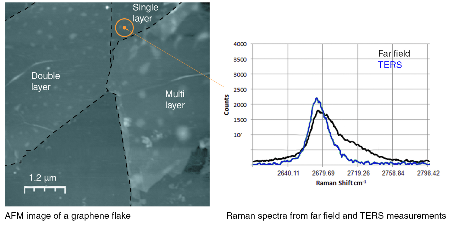
Tip-enhanced Raman scattering (TERS) is a type of SERS which uses a metallic-coated tip to enhance the Raman signal. The TERS technique boosts the Raman signal from molecules within a few nanometres of the tip. This method can resolve nanometre-sized particles. For comparison, the diffraction-limited spatial resolution of conventional far-field Raman scattering is >0.2 μm.
We can use TERS for super-resolution chemical imaging. We can achieve this by comparing the spectrum from the sample surface with and without the tip present. The TERS tip is typically mounted on a scanning probe microscope (SPM) or atomic force microscope (AFM). Renishaw's inVia Raman microscope can perform in-situ SPM/AFM measurements, including TERS.
Renishaw's combined Raman-SPM/AFM is available with TERS options.

AFM image of a graphene flake with Raman spectra from far-field and TERS measurements. The TERS Raman spectrum easily resolves the small region of single-layer graphene. The far-field Raman spectrum has a broader 2D band, showing some contribution from the nearby double-layer graphene.
What is Raman spectroscopy?
Continue your exploration of Raman and photoluminescence (PL) spectroscopy. We answer your questions on Raman microscopy, fast Raman imaging, data analysis, fluorescence and complementary analytical techniques.
Raman spectroscopy explained