Denna sida finns för närvarande inte på ditt språk. Du kan
översätta
den automatiskt
med Google Translate. Vi ansvarar inte för att tillhandahålla denna tjänst och
vi har inte kontrollerat översättningsresultaten.
Kontakta oss om du behöver ytterligare hjälp.
Semiconductor analysis with Raman spectroscopy
Modern electronics use a wide range of semiconductor materials. Cutting edge devices, such as transistors, solar cells and light emitting diodes, push materials properties to their limits, and require extremely homogeneous source materials. Raman spectroscopy is an ideal tool for studying semiconductors.
Characterise semiconductors
You can use Raman to characterise and generate images of all semiconductors (e.g. Si, carbon-based, III-V's, and polymers) and superconductors. A wide range of information can be revealed, including:
- chemical composition (e.g. alloy fractions of compound semiconductors)
- polytypes (e.g. 4H-SiC and 6H-SicC)
- strain/stress
- dopant concentrations
- thin film thickness
- crystal structure type and orientation
- crystal quality
- uniformity and purity
- device temperature

Easy analysis
Raman analysis is simple because it requires no sample preparation. It does not require vacuum technology, or suffer from charging effects experienced with electron microscopy.
Renishaw can configure your Raman system to suit all users, from research scientists to technicians.
Large area analysis
Renishaw Raman systems can analyse very large samples. For example, you can generate images of entire wafers to discover contaminants or residual stresses.
PL characterisation
Renishaw's Raman systems also enable you to collect and analyse photoluminescence (PL) spectra. You can collect both vibrational and electronic information with one instrument.
Online systems
Add Renishaw's Raman systems to your production line to conduct online analysis for quality control purposes. Diagnose problems early, reduce waste and improve yield.
Reliable results
Renishaw's Raman systems produce highly repeatable data that accurately represents the sample. In-built automated calibration and health checking ensure data can be accurately compared, no matter when collected.
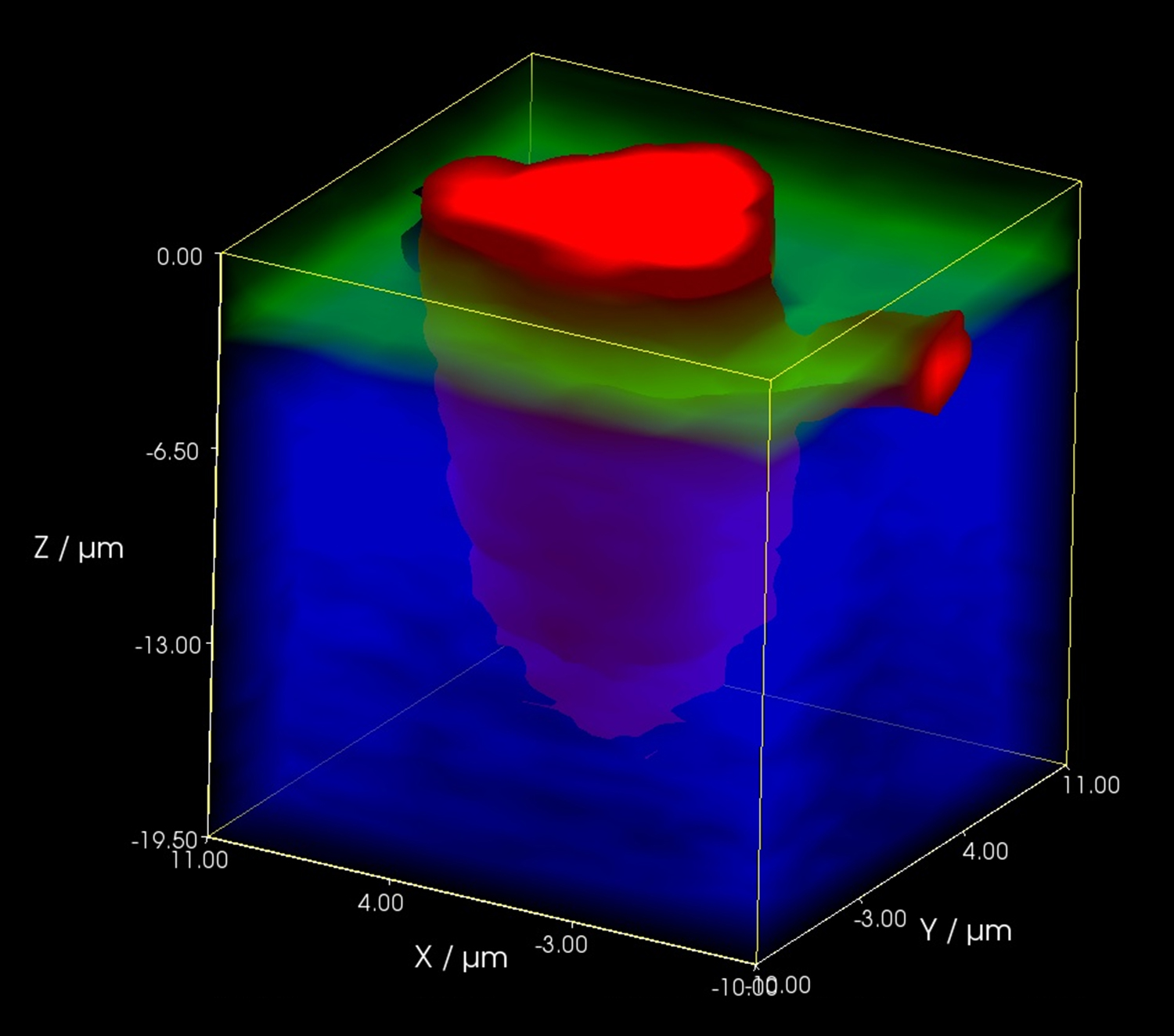
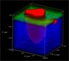
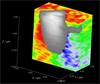
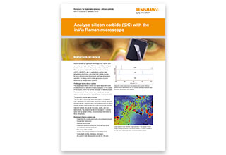
3D Raman map of a Silicon Carbide wafer

We're here when you need us
To find out more about this application area, or an application that isn't covered here, contact our applications team.
Contact our applications team
Download document
Related stories
Combined MWIR Raman thermography for improved thermal control in semiconductor devices
Thermography microscopes can efficiently map high-temperature zones over large surface areas, but the challenge is being able to pinpoint minute areas of high heat. To address this, Quantum Focus Instruments (QFI) coupled a Renishaw Virsa Raman analyser to their InfraScope, enabling interesting Raman thermographic findings.
Caltech working to solve the world's energy problems with the help of inVia
The California Institute of Technology (Caltech) is on a mission to find new and effective ways to produce solar fuels using only sunlight, water and carbon dioxide. A focus of this is investigating photocatalysis and light capture.