No momento esta página não está disponível em seu idioma. Você pode ver uma tradução automatizada utilizando o Google Translate. Não somos responsáveis pelo fornecimento deste serviço e não podemos verificar os resultados.
Se você necessitar mais ajuda fale conosco.
Case study: Combined MWIR Raman thermography for improved thermal control in semiconductor devices
Background
Quantum Focus Instruments Corporation (QFI) supply world-leading temperature measurement microscope systems for the semiconductor industry. Their systems collect critical data to the reliability and thermal management concerns of engineers working across application areas including space, radar, communication, and power conversion. Identifying areas of high temperature within a semiconductor device helps designers to achieve better and long-lasting performance.
Using a QFI infrared (IR) thermography microscope, high-temperature zones can be efficiently mapped over large surface areas, but the challenge is being able to pinpoint minute areas of high heat. The higher spatial resolution of the Renishaw VirsaTM Raman analyser can resolve smaller areas of peak device temperature. This technique is called Raman thermography.
What is Raman thermography?
Raman thermography (or Raman thermometry) uses the Raman spectrum from a semiconductor device to determine the local temperature with submicron lateral spatial resolution. When a transparent layered semiconductor device is sampled using Raman spectroscopy, characteristic phonons are observed for each material in the structure. Raman thermography uses the temperature-sensitive change in phonon frequency to measure the temperature of a material. Raman thermography can be readily applied to devices fabricated from silicon, gallium nitride (GaN), and gallium arsenide (GaAs).
The combined MWIR Raman thermography system
The Renishaw VirsaTM Raman analyser is a versatile fibre-coupled system which can be easily combined with other analytical instruments. In this example, a Virsa analyser has been coupled to a QFI InfraScopeTM, an established mid-wave infrared (MWIR) temperature measurement microscope. This combined system is designed for the accurate determination of temperature in the layers of a device's structure. Figure 1 shows the combined MWIR Raman thermography system in use.
Combined thermography measurements were conducted on a commercially manufactured GaN high-electron mobility transistor (HEMT). MWIR measurements were taken from the whole device to find regions of peak temperature, as shown in Figure 2. Next, the coupled Virsa analyser enabled high-resolution Raman thermography from the highlighted region of peak temperature.
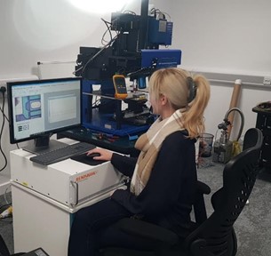
Figure 1 | A researcher inspects a semiconductor device with a Renishaw Virsa Raman analyser coupled to a QFI InfraScope.
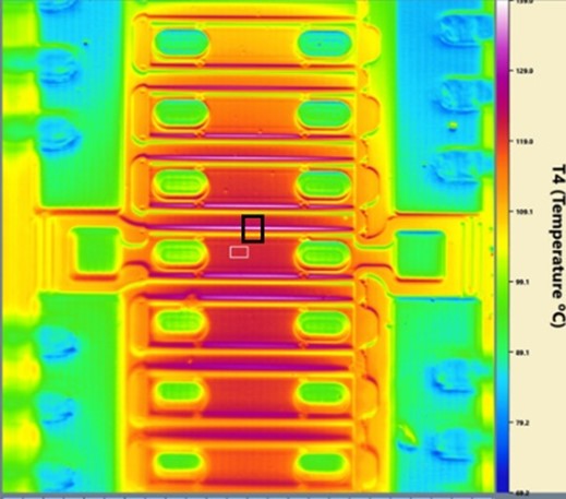
Figure 2 | MWIR thermography image showing the temperature distribution in a GaN HEMT. The black rectangle marks the area of peak temperature, which is then analysed using high-resolution Raman thermography.
"The integration of the Renishaw Virsa probe into our InfraScope further enhances our ability to measure highly differentiated temperature gradients in the lateral and vertical axis of semiconductor devices and materials." - Paul Hayes, applications manager QFI
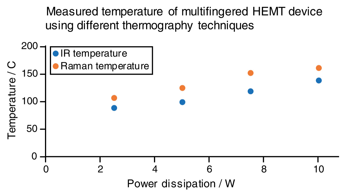
Figure 3 | Comparison of measured MWIR and Raman thermography temperatures for a multi-fingered GaN HEMT device at different operating powers. The higher temperatures recorded by Raman thermography can be attributed to higher spatial resolution, and thus a more accurate reading of peak device temperatures.
Results
Figure 3 compares the GaN HEMT device temperatures measured using MWIR and Raman thermography techniques at different operating powers. MWIR thermography records temperatures that are about 20% lower than those measured by Raman thermography. When looking at a bulk hot source, both thermography techniques produce the same temperature, and no discrepancy is observed. This discrepancy can be attributed to the higher spatial resolution of the Raman technique giving a more exact measurement of the high temperature region. Therefore, the Raman measurements are more representative of the peak device temperatures and thus more useful for characterising the device and modelling its lifetime.
Summary
Integrating a Renishaw Virsa analyser and a QFI InfraScope shows the power of combining the speed of MWIR thermography with the higher spatial resolution of Raman thermography. This could be an invaluable tool for the ongoing development and commercialisation of semiconductor materials such as GaN high electron mobility transistors (HEMTs).
More about QFI
If you would like to find out more about QFIs microscope systems for the semiconductor industry, follow this link to their website:

Further reading
We have a whole range or articles, case studies and news stories about Raman spectroscopy.
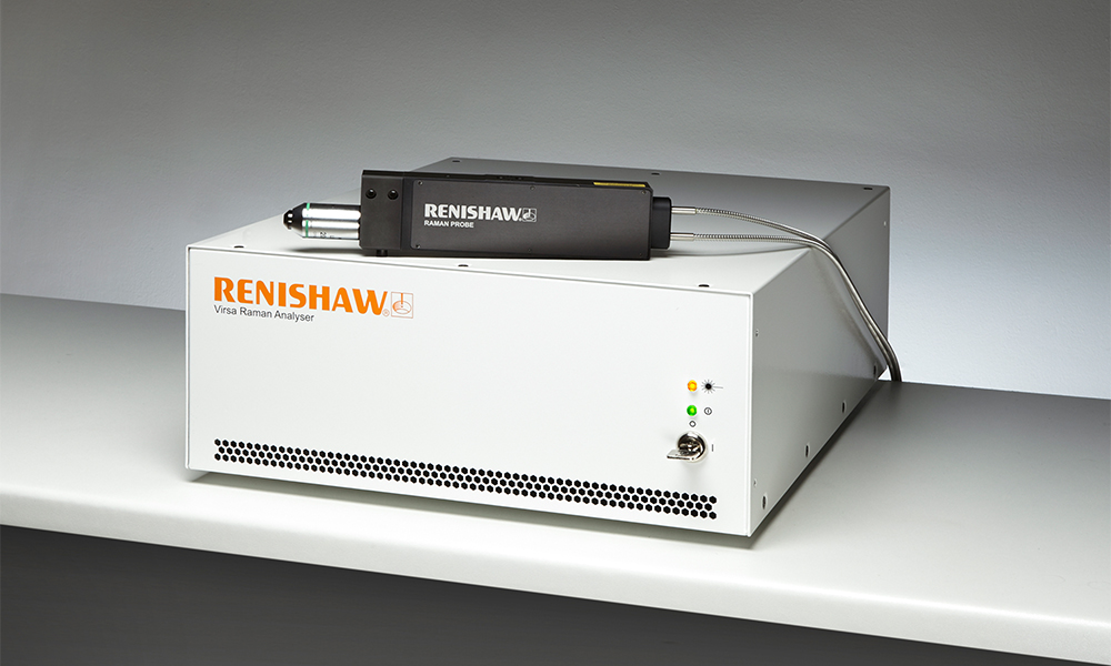
About the Virsa Raman analyser
Discover more about how the Virsa Raman analyser is suitable for your organisation's applications.